Fermi Level In Semiconductor : Answered 37 O Doping Changes The Fermi Energy Bartleby : The fermi level is referred to as the electron chemical potential in other contexts.
Fermi Level In Semiconductor : Answered 37 O Doping Changes The Fermi Energy Bartleby : The fermi level is referred to as the electron chemical potential in other contexts.. At higher temperature one finds that the transition between completely filled states and completely empty states is gradual rather than abrupt. In metals, the fermi level lies in the hypothetical conduction band giving rise to free conduction electrons. No states above the fermi level are filled. The fermi level plays an important role in the band theory of solids. When many li atoms, for example, form a solid, the individual.
Na is the concentration of acceptor atoms Whenever the system is at the fermi level, the population n is equal to 1/2. Fermi level of a semiconductor for insulators, the energy gap is large enough so that the fermi level lies far from the conduction band or states that can carry current. Therefore, the fermi level for the intrinsic semiconductor lies in the middle of forbidden band. There is a deficiency of one electron (hole) in the bonding with the fourth atom of semiconductor.
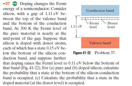
Answered 37 O Doping Changes The Fermi Energy Bartleby from prod-qna-question-images.s3.amazonaws.com At the interface, you should expect a lot of these surface states or interface states producing these energy levels within the band gap located physically at the interface. The fermi level is at e / u = 1 and k t = u. In this case the fermi level is defined as the level in which the probability of occupation of electron at that energy is ½. For example, in li, the two 1s orbits are filled, while there is 1 electron is there in the 2s shell. The electrical conductivity of the semiconductor depends upon the total no of electrons moved to the conduction band from the valence band. Fermi level of intrinsic semiconductor. Whenever the system is at the fermi level, the population n is equal to 1/2. The fermi energy is defined as:
The fermi level plays an important role in the band theory of solids.
If you can bring the fermi level high enough, then part of the tail will go over to the conduction band. Fermi level lies in the midway between the valence band top and conduction band bottom of an intrinsic semiconductor, as shown in fig. In metals, the fermi level lies in the hypothetical conduction band giving rise to free conduction electrons. Energy level of conduction band consists of the electrons which are responsible for conduction. At the interface, you should expect a lot of these surface states or interface states producing these energy levels within the band gap located physically at the interface. If the temperature will be maintained at. Na is the concentration of acceptor atoms 1.1 0, indicating equal concentrations of electrons and holes. The highest energy level that an electron can occupy at the absolute zero temperature is known as the fermi level. The fermi level lies between the valence band and conduction band because at absolute zero temperature the electrons are all in the lowest energy state. Fermi level is a kind of measure of equilibrium electronic energy of a solid material. Fermi level of metal and semiconductors: The value for the fermi energy and carrier density is obtained at the crossing (indicated by the arrow) of the two black curves which represent the total positive and total negative charge in the semiconductor.
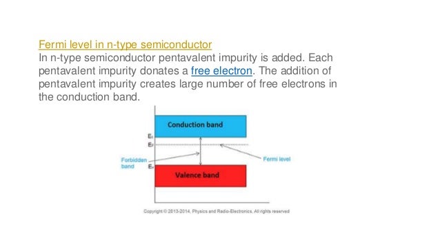
As you know, in an atom, certain energy levels are filled, while others are empty. (a) fermi level position in pure semiconductors at this point, we should comment further on the position of the fermi level relative to the energy bands of the semiconductor. Whenever the system is at the fermi level, the population n is equal to 1/2. However, in semiconductors the bands are near enough to the fermi level to be thermally populated with electrons or holes. In semiconductors the position of the fermi level is within the band gap, approximately in the middle of the band gap.
Fermi Level In Extrinsic Semiconductor from image.slidesharecdn.com This definition of fermi energy is valid only for the system in which electrons are free (metals or superconductor), or any system. Fermi level is a kind of measure of equilibrium electronic energy of a solid material. The fermi level is the level where the probability that an electron occupies the state is 0.5, e.g. 1.1 0, indicating equal concentrations of electrons and holes. But in the case of a semiconductor there is no allowed energy level between the valence band and. In this case the fermi level is defined as the level in which the probability of occupation of electron at that energy is ½. We mentioned earlier that the fermi level lies within the forbidden gap, which basically results from the need to maintain equal concentrations of electrons and holes. Whenever the system is at the fermi level, the population n is equal to 1/2.
Fig.2.7.2 graphical solution of the fermi energy based on the general analysis.
In this video, the concept of fermi energy/ fermi level is discussed for intrinsic semiconductors. Na is the concentration of acceptor atoms. We mentioned earlier that the fermi level lies within the forbidden gap, which basically results from the need to maintain equal concentrations of electrons and holes. No states above the fermi level are filled. The value for the fermi energy and carrier density is obtained at the crossing (indicated by the arrow) of the two black curves which represent the total positive and total negative charge in the semiconductor. Fermi level is the highest energy level occupied by the electrons in the material at absolute zero temperature. So, let's consider these fermi level pinning effect in the schottky contact. Due to this, a hole is created in the adjacent atom. It's an interface between two different materials semiconductor and metal. I can understand that the distribution changes with the temperatures (it gets broader) but i don't understand why/how the fermi level changes. The electrical conductivity of the semiconductor depends upon the total no of electrons moved to the conduction band from the valence band. If you can bring the fermi level high enough, then part of the tail will go over to the conduction band. About press copyright contact us creators advertise developers terms privacy policy & safety how youtube works test new features press copyright contact us creators.
These electrons jumps up from the valence shell and becomes free. Where the fermi energy is located (correct?). Whenever the system is at the fermi level, the population n is equal to 1/2. The fermi function which describes this Na is the concentration of acceptor atoms
Doping Of Semiconductors And Fermi Energy Physics Forums from www.physicsforums.com The opposite is true for conductors where the fermi level is within a band or nearby states that readily carry current. Fermi levelis the state for which there is a 50% probability of occupation. If the temperature will be maintained at. Fermi level in the middle of forbidden band indicates equal concentration of free electrons and holes. Energy level of conduction band consists of the electrons which are responsible for conduction. Where the fermi energy is located (correct?). The fermi function which describes this Fermi level of a semiconductor for insulators, the energy gap is large enough so that the fermi level lies far from the conduction band or states that can carry current.
This definition of fermi energy is valid only for the system in which electrons are free (metals or superconductor), or any system.
In this case the fermi level is defined as the level in which the probability of occupation of electron at that energy is ½. Fermi level is the highest energy level occupied by the electrons in the material at absolute zero temperature. Fermi level of a semiconductor for insulators, the energy gap is large enough so that the fermi level lies far from the conduction band or states that can carry current. The value for the fermi energy and carrier density is obtained at the crossing (indicated by the arrow) of the two black curves which represent the total positive and total negative charge in the semiconductor. If the temperature will be maintained at. In insulators and semiconductors the fermi level is inside a band gap; Fig.2.7.2 graphical solution of the fermi energy based on the general analysis. Fermi level lies in the midway between the valence band top and conduction band bottom of an intrinsic semiconductor, as shown in fig. At higher temperature one finds that the transition between completely filled states and completely empty states is gradual rather than abrupt. Where the fermi energy is located (correct?). The fermi level plays an important role in the band theory of solids. In semiconductors the position of the fermi level is within the band gap, approximately in the middle of the band gap. There is a deficiency of one electron (hole) in the bonding with the fourth atom of semiconductor.


0 Komentar